Showing posts with label Guide. Show all posts

Friday, 5 September 2014

Test box 2.0

We always recommend trying the boards out before soldering everything in to the enclosure. Main reason being that if you have an error on your build, it's about a hundred times harder to find it inside the otherwise finished build. Like Madbean says - Build it, Rock it, Box it. There is a reason for that order. One could, of course, simply use a breadboard and/or simple screw terminals to achieve the same goal, but if you are building more than one circuit every now and then.. Well. Then i'd suggest you'd build yourself a test box. I've had a few different methods of trying the boards out before boxing, but my latest, equipped with a little more sophisticated screw terminal block was closing in on the end of the road. It was simply falling apart due all the use it had seen. So. I wanted to build myself a new one with slightly more features than the previous one. And while i was at it, i snapped a few (poor) shots of the process. A slight warning: This "photo essay" may not be detailed enough for someone who's doing anything like this for the first time. But if you know what you're doing, you're more than welcome to try something similar out. Here's my "Test box 2.0", which includes a switchable audio probe input. Let's start out with what you'll need.


Most things needed are your standard pedal parts.
  • Enclosure (i used a plastic box that can be found through Tayda)
  • 4-way speaker terminal and bolts/nuts for it (again, Tayda)
  • 2 mono jacks
  • Binding post for "banana" connector (mine isn't exactly like this, but once again - Tayda)
  • 3PDT On-On toggle switch
  • DPDT On-On toggle switch
  • 1µ polyester box capacitor (higher the voltage rating, the better)
  • Small piece of stripboard
  • 2 LEDs (i used diffused red and orange)
  • 2 1K2 resistors for the LEDs
  • Holders for the LEDs
  • A few meters of wire of your choice
  • Heat shrink tube etc. etc.
I drilled the enclosure first and started with mounting all the ingredients. Due to location of everything on my bench, i went with jacks on the left, speaker terminals on the right, DC jack on top and probe binding post at the bottom. I Placed the switches on the upper half, because it just looked like that would be a good place for them. The LED holders are below the switches. You should probably think the geometry of all the parts so that it'll suit your needs and bench.


Next up, we'll wire the grounds. The DC jack pictured here has its longer leg as sleeve and shorter as tip, so we'll take a wire from the short one to lug 2 of the DPDT switch - and from that pin to the second speaker terminal lug - and from that to input jack's sleeve - and from that to output jack's sleeve - and from that to lugs 1, 4 and 5 of the 3PDT switch. Here's picture of all the grounds connected:


Now, the small piece of vero. We're using that as a tiny daughter board for our LED resistors, just to keep everything neat. 4x5 board is enough. We'll wire two red wires to one row with two resistors and one wire for each row that has the other end of the resistor. Those wires are for the LED anodes. Like so:


Now we can wire up all the "hot" leads inside the box. To attach the tiny board to the enclosure, i used Tesa PowerBond Outdoor branded two sided adhesive tape. 3M's similar product doesn't insulate the connections, so do not use that. With slightly bigger board one could use a plastic, or even metal PCB standoffs, but i've found the Tesa tape to be sufficient solution. LEDs go their respective holders (i'm using red for bypass/3PDT and orange for probe/DPDT) and cathodes need to be soldered to lug 3 of the DPDT and lug 6 of the 3PDT. The longer free red wire goes to DC jack's sleeve and the shorter to the first speaker terminal lug.


Now we have all the grounds and supply wires hooked up. Next we'll need to solder up the signal wires. Connections are pretty much per the standard outboard wiring, but please do read this twice to make sure you got it:
  • Green wire - from 3PDT lug 2 to speaker terminal lug 4
  • Blue wire - from speaker terminal lug 3 to 3PDT lug 9
  • Yellow wire - from input jack's tip to 3PDT lugs 3 & 7
  • Orange wire - from 3PDT lug 8 to DPDT lug 4
  • Brown wire - from DPDT lug 5 to output jack's tip
All that wiring is depicted here:


We're pretty much all set, but the probe section is still missing. The box does work as it is now, but there's no use for the binding post and the DPDT switch does nothing - but light up the LED when set to probe mode. Now we'll need to solder two wires to the 1µ capacitor. Like this:


Other end of that wire is then fastened to the screw at the bottom of the binding post. The other end needs to be soldered to DPDT lug 6. I used a small piece of the two sided adhesive tape to keep the capacitor nicely in one place. Like so:


That's it. Simple and straight forward. The 3PDT bypass switch acts as a true bypass in the same manner as in any pedal. The speaker terminal connections are the ones where you'll snap in your just finished new effect board. One for supply voltage, one for ground, one for circuit input and one for circuit output. Here's a shot of the thing in action:


Some of you may think "why add the binding post for the probe?" Here's the reason - let's assume i've built a board, hooked it up to this box and it doesn't work. There's no signal passing through. We already have the ground wire for the circuit connected, so why should we rip out all the cables (excluding the supply/ground) and clamp an alligator clip to a ground point on circuit, plug the probe to the amp and start probing? For no reason. With this setup, we can simply connect a multimeter's test lead to the binding post, flick the probe switch and start probing. Even when debugging a broken factory pedal, this solution eliminates the need for a separate probe. Just connect that pedal's grounds to the ground slot of the speaker terminal and start probing.

How am i going to remember which of the speaker terminal slots is which and which jack is which? I'm probably not going to, so. I added some Dymo tape to mine...


I = Input, O = Output, G = Grounds and V = voltage in. Don't bother pointing out that the speaker terminal is upside down. It isn't. This way i can snap the wires in without having to lift the box off the table.

The idea for this box is rather simple and you should be able to add the features you want/need. Like for example - a negative charge pump and separate 2-way speaker terminal for the -9V and ground. That feature would enable you to try out positive ground circuits with the same test box. Why i'm not doing that? Because i have a lab supply on my bench and i want to be able to try the circuits out with higher voltages than just 9V. So ICL7660S with maximum input of 12V doesn't really suit my purpose.

One last thing. If you don't have a lab power supply with quick fuse, please do not test your circuits with a wall wart power supply. Even the slightest short will burn your supply or its regulator in a heartbeat. For testing purposes - solder a standard DC plug to a battery snap and go with that. You'll be able to drain a battery in ten seconds with a short, but it'll be a lot cheaper than burning wall socket adapters.

Wednesday, 13 August 2014

Negative and Positive Ground Effects


This question comes up frequently and many of the articles you read about it online can be a little difficult to get your head around sometimes, so I thought I'd just do a short write up on negative and positive ground effects and the problems associated with mixing them.  I am writing this in a way that I think will be easy to understand, but if I over simplify or miss out anything important then by all means post in the comments and I will edit where necessary :o)

One thing that makes this topic confusing for some is that we can often think of the supply having a +9V positive side and a 0V negative, but although this is often perceived to be true, it isn't exactly the case.  With a floating supply like from a battery or isolated power supply there is no point of reference until it is in a circuit and so the only thing we know for sure is that the positive side is 9V greater in potential than the negative.  In a common negative ground effect this makes perfect sense to us, ground is 0V and the positive supply is +9V, but when we build an effect and are instructed to connect what we think of as the +9V side to ground it doesn't compute.

When you have a chain of effects, ground is fixed at 0V by the negative ground effects, and more importantly your amp which is connected to all effect grounds via the sleeves of the connecting cables.  So that "9V connection" to ground you made in your positive ground build is set at 0V by the local connections.  This gives a reference point for the supply, and remembering the negative side going to the supply point of the effect circuit is 9V lower, that determines it must be -9V.  This is why it is never a problem to mix negative and positive ground effects in your chain.  Ground is always 0V with each pedal having either a +9V or -9V supply when in circuit depending whether the ground connection has used the negative or positive side of the source of supply. 

The problem with mixing negative and positive ground effects comes when people try to power them with the same source of supply.  In this instance the power supply isn't floating any more, negative is 0V and the positive is 9V and so making that non-computing connection from positive to ground creates an immediate short which will usually destroy your power supply unless you have one with a fuse or some other sort of short circuit protection.

So what can you do?

This is why power supplies with multiple isolated outputs can be very useful.  Because the channels are isolated from each other, they find their point of reference independently and so you can have one powering negative ground effects at 0 to 9V and the other isolated side powering positive ground effects at -9 to 0V.  Then there is no problem in daisy chaining all your positive ground pedals together from one isolated output channel, and likewise daisy chaining all your negative ground pedals together from another.  Always ensuring of course that the current available from each output isn't exceeded by the pedals' combined consumption.

As an alternative, and something I always recommend trying with the layouts on this site is to use a charge pump IC to provide a negative voltage.  The charge pump takes a 9V input and gives a -9V output, so instead of connecting the positive side of the supply to ground this allows you to keep all ground connections 0V, and supply the positive ground effect with the -9V from the charge pump.  Common ground, common power supply.

Friday, 2 November 2012

Components

Part 2 of the component guide by Miro, this time looking at active components.  A good read particularly for someone new to the hobby may have a lot of his questions answered.


Part One   |  Part Two


Builder's components, part two - Active components

Good day to you all. This article here is the part two of my component tutorial, aimed for the beginner builders. I've already disclosed the reasons why i'm doing this in the first part of the series. If you're asking me how many volumes i'll write; i really don't know. When i run out of steam i suppose.

Anyway. Let's start with diodes of all types and go on to the transistors.


Diodes

Diodes aren't exactly active components in meaning of the word, but they still are semiconductors. Where resistors slow down the current, diodes can do the same to voltage. But they can do more. We have a few different types of diodes, and they all have their own purposes on the circuits. From light emitting diodes to standard switching diodes to schottkys and zeners and so on. Wikipedia entry for diodes shows the magic-like list of all the different types imaginable. All diodes have anode and cathode. Laymans terms, the anode is positive and cathode is negative side. So if you will, these are polarized in the same manner as polarized caps. We'll be mostly needing LEDs, schottkys and switching diodes for our builds. But let's not get ahead of ourselves.

LED - Light Emitting Diode

LEDs are diodes too. Hence the name. We have usually two different purposes for the LEDs in our circuits - First, we use LEDs outside the boxes to tell us when the pedal is on. Other viable and common use is to clip the signal with LEDs. If you see two LEDs on a board, connected back to back, then that's the clipping stage created with LEDs. They come in variety of sizes, shapes and colours. Most common are round 3mm and 5mm LEDs. There are 8mm and 10mm round LEDs available too. And the LEDs come in various packages, or shapes, like square style, short hat... Note that the longer leg is always the anode (the positive, "+" side) and the shorter is cathode (the negative, "-" side).

You can find a vast variety of different colours, diffused and "water clear". Clear ones are usually brighter, and they usually need higher resistance to produce same ammount of light than diffused ones. By the way, the resistance between power souce and the anode (or in some cases, cathode and ground) means how bright or dim the LED is once it's on. Diffused ones are coloured and clear ones are just transparent, no matter what's the colour when it is on. You can find red, green, yellow, pink, white, blue, orange and more as diffused and clear. Note that usually the pink, white and blue are more expensive than red, green and yellow. There are good(ish) starter packs out there, but usually their prices can be beaten by just checkin some cheap part store like Tayda. You probably want to have many different colours in stock.

Well. We also have multicoloured and other special LEDs out there. These have either common cathode or common anode. Which you might need depends on where you're going to use them. And how. One purpose would be to use two coloured LED as indicator in build where you may have two circuits in a single box. That would need common anode type. Anode feeds the current for both colours and two anodes go to their respective switches to be connected to ground. But. I bet there's enough to learn with basic LEDs as these are much more often used in our purposes.

It may be good to start with stocking up on your favourite colours in 3mm and 5mm, diffused or not, that's, of course, based on what you like.

As i mentioned above, LEDs are also commonly used as clipping diodes. Different colours have different and distinct tonal differences. Colour makes more difference than the size than shape of the LED. You can always socket the two back to back clipping diodes on your build and try out different combinations. For example, red and blue sound completely different. That's one more thing to try out.

*Hint: Try out one red LED straight on to a 9V battery. Longer leg to plus terminal and shorter to minus. This experiment will cost you one 2-3 cent LED, but you'll never forget to use a resistor between the power source and the LED.

General use diodes

Switching diodes and schottkys are the most common in our builds. For basic silicon clipping, we'll want 1N4148 switching diode. These are cheap and commonly used diodes. I think it's good to know that 1N4148 and 1N914 are the same thing. 1N4148 replaced its leakier predecessor 1N914 some decades ago. But. Now if you buy 1N914, it's going to be exactly the same as 1N4148, just marked as 1N914. Internet tells us that manufacturers do this because there is still demand for 1N914 due to mass of perfectly good and usable schematics from past decades. But they are still the same as 1N4148s. Unless you can dig up some really old NOS 1n914s...

Many designs use 1N5817 or 1N4001 schottkys as polarity protection. You might want to stock up on those too. The latter drops more of the voltage than the former. But former costs a lot more in comparison. If schematic or layout has 1N5817 in it, you can safely use 1N4001 in its place. In theory, all barrier schottkys are meant to pass the current 1:1 on the "right" direction and stop the current from passing in the wrong direction completely. This is the basic operation of all diodes.

Ah, but then we have all the magic diodes. Germanium diodes, like 1N34A, 1N270, OA91 and super lenghty list of others. The list goes on forever. Foe example, 1N60Ps are quite cheap and they are good to have. Others.. Well. A diode is a diode is a diode. For clipping stages, you'll get tonal differences with different diodes, but the rule of thumb is that germanium diodes will always be more quiet than their silicon counterpart. Germanium diodes cost roughly at least seven times what modern silicon diodes cost. And for NOS, the prices go through the roof. If the design has two 1N270s (like, for example, in DOD OD250) in it, you won't be totally off by swapping them with two 1N4148s. It won't sound 1:1 with the original, but i can promise you that this is something you will want to try eventually.

Some designs use zener diodes. These are more special cases. I personally don't see the point in sourcing and stocking all the possible values from 1V to 36V and beyound, as you'll probably need just 4,3V or 4,7V, 5,1V and 9,1V zeners in your first year(s) of building. It's really rare that some application needs exactly 4,7V zener - in my experience, the circuit will work fine with 5,1V zener in it's place. So just like with the humble resistors, you can always use the closest value you have at hand.

All of the above are marked with a stripe, regardless of the package. The stripe marks the cathode side of the diode. Did you already forget? Cathode is the negative (-) side of the diode. It's the anode that is positive.

As diodes go, they are generally somewhat cheap components and easy to stock up on due to wide availability. So, in addition to LEDs, you'll need at least a fair batch of 1N4148s and 1N4001s. In addition, some zeners won't hurt you. But you could always stock up on all of them..


The almighty Transistor

Now we're getting to the point where the real magic happens. Well. It's not that much of a magic than just plain good old physics. Transistors are used to amplify the current - which in this case is our signal. All transistors work in the same general principle - turning signal's current to stronger current with help of voltage, bias voltage and ground. This is the point where i urge you to always check the datasheet. It's easy. Just fire up google or any other search engine and type in the model of the transistor and a word "datasheet". Once you've done that several times on one particular transistor, you'll start to remember stuff like the pinout and hFE (which is the number that tell us about the transistors real gain).

Ok. Transistors are discrete devices that can amplify our signal. There are too many models and too many little differences between them to list them all. But the things we need to know are that we are commonly using BJTs (bipolar junction transistors), which is just referred to as, well, the transistor. Then we have MOSFETs and JFETs. Those are the most common three.


Bipolar Junction Transistors

Or the transistor. It has always three legs. One is called the collector, one is called the base and one is called the emitter. That's at least three legs. Transistors with four legs and some other special ones with two bases exist too. Usually we're going to need the basic ones with pinout like emitter-base-collector or base-collector-emitter.

One great discovery happened when former me ordered a silicon fuzz face kit. Former me opened bag and was baffled. "Did they mistakenly send the wrong transistors? Are these germanium instead of the silicon i ordered? I don't know what to do!?". Check the datasheet you idiot. Silicon bipolar junction transistors come in variety of packages. The metal can does not automatically mean that the device is germanium (i'll tell you more about the germs later). 2N2222 come in TO-18 package, which is metal can. BC108, BC109, 2N2907 and massive amount of others come in TO-18 as well. And they all are silicon devices. Normal black plastic package, the TO-92 is used in more devices though. Metal can gives the mojo feeling to a transistor. In case of 2N2222(A), you can get both packages, the TO-18 and TO-92, and it's still exactly the same device. There are others like this too.

Well of course the transistor catalogue of you local electronics shop is quite different from what it was 30 years ago. But the transistor is still just a transistor. To begin with, you should source the most widely used cheap transistors. It doesn't matter what the original schematic says, if it uses BJT (that's Bipolar Junction Transistor), then any BJT will do the job. It probably won't sound exactly 1:1 with the original, but will it sound worse? If the hFE range is the same, then probably not. The basic, most widely used transistors, and thus making a good sourcing tip, would be:
-2N2222(A) (BJT NPN +75 hFE)
-2N3904 (BJT NPN ~300 hFE)
-2N5088 (BJT NPN 400-800 hFE)
-2N5089 (BJT NPN low-noise 500-1200 hFE)
-2N2907 (BJT PNP +70 hFE)
-2N3906 (BJT PNP ~250 hFE)
With batch of each one of those, you'll be able to build almost any circuit that uses bipolar junction transistor. (Heh. If some of the hFEs are not 100% correct, please remember that i didn't check any datasheets for writing that information. I just grabbed the hFEs from my brain's memory banks.)

Now.. What's the deal with NPN and PNP? Doesn't that make all this a bit complicated? Yeah. I guess it does. At the beginning of the building hobby it surely does. Well it's quite simple after all. It is affected by the direction of the current. That's why normally we'll need negative 9V with circuits that are using PNPs. This is one of those things that is slightly too complicated to unleash on a beginner. Anyway, I suggest that you familiarise yourself with NPN transistors and negative ground builds until you are sure you can take on PNP designs.

*Hint: Build yourself a silicon Fuzz Face clone with two 2N3904s. That way your parts on the board will cost you less than 15 cents. That doesn't include the board material, pots, wires, footswitch, nor that possible trimpot. And it won't sound anywhere near the classic germanium AC128 Fuzz Face. But. The parts for the board still cost you less than 15 cents.

NPN and PNP is the same thing with germanium transistors. Germaniums are currently used in pedals and not much elsewhere. They leak current. Even the best ones do. That's the fault that guitar effect designers have used for their advantage since the sixties. Plus the fact that silicon devices, invented in 1954, were expensive at the time. That's the main reason guitar effects used germanium transistors for so long. Then you might ask why most of the germanium circuits are PNP? Well. History has it that most PNP germanium device models were much more consistent than their NPN counterparts. NPN germaniums exist. Good ones are just mostly gone. If you check the ebay for NPN germaniums, there are some, but they cost a lot more than PNPs of the same gain range. I've hoarded some germanium transistors, and i can tell you that none of the germanium transistors are consistant enough to just take from the bag and rock. It never works that way. Only measuring the gain and compensating the leakage in that measurement can lead to working germanium build.

Anyway. Good way to start out would probably be with the common NPN bipolar junction transistors and when you feel ready, then get your hands dirty with PNP and germaniums. Germs sound amazing due to their faults, but you may have to pay up to 500 times more for basically inferior device.

Always check the datasheet. That is the one message i can't repeat enough. What we want to know from them are just a) The pinout, and b) hFE=gain range. Those two are the ones you'll need over and over again. There is always way too much information on those documents, but you will manage fine with those two pieces of information.

*Hint: If fyou store all your different transistors in small plastic bags (like i do), you could write the basic information you'll need on the bags. Like for my bag of 2N3904s: NPN - EBC - ~300. Then i know straight away the pinout and general range of hFE.

Another type of BJT is the Darlington. Darlington is a device that basically has two normal BJTs piggybacking inside one transistor box. That configuration can lead to massive gains, like 20000 (twenty-thousand) hFE. Some manufacturers, like Devi Ever and Death by Audio seem to be in love with these. Basic two models would be 2N5306 and MPSA13. Both good sourcing targets. Wikipedia has nice article about the Darlington configuration that explains a lot. Just a hint for those who are interested.


Field Effect Transistors

JFETs and MOSFETs? Why on earth we do have so many different types of transistors? Well, the operation is quite different between bipolar junction transistors and field effect transistors. More importantly, the sound is completely different due to different bandwidth. FETs alledgedly sound nearly like tubes. That is not completely off, as you can get tube-like sound from these transistors and they were supposed to be solid state replacement for tubes to begin with... In harsh reality, only thing that sounds exactly lika a tube is a tube. FET's operation is based on electric fields, but that's a bit steep for now.. FET is older invention than BJT, but mass manufacturing of these devices started some time after BJTs. So, FET stands for Field-Effect Transistor and MOSFET for Metal Oxide Semiconductor Field-Effect Transistor. MOSFETs are notoriously delicate to high voltages. Even simple static charge can kill the device, so handle those with care. Pins of a FET are called the Drain, Gate and Source. Those translate loosely to drain being like the collector, gate like the base and source being like the emitter on a BJT. Usually the pinouts are drain-gate-source and gate-drain-source. Like i said above, the characteristics of a FET make it sound much more like the vacuum tube than squeeky clean counterpart, the BJT. FETs do not have hFE to tell you the gain. That is listed as IDSS and GFS in their datasheets. Those translate to current being put out by the transistor.

Basic and the most popular devices are without a doubt 2N5457, 2N5458, J201, MPF102, 2N7000 and 2N5259. There is much much more to FETs, as this is just a short introduction. FETs sound amazing in many applications and they are somewhere between germanium and silicon BJT when it comes to ease of use - Silicon BJT being the simplest and easiest device to build circuits with.

FETs can be used for clipping too. You could try them with source as anode and gate + drain as cathode. This will result in soft clipping. Once again, tube-like soft clipping.

There is a huge number of different types of transistors out there. Radio frequency and microwave. Exotic semiconducting composite materials, like hybrids between silicon and germanium and so on. And while we do use them mainly for amplifying guitar or bass signals, they can be used for other purposes too - like electronic switching.

*Hint: The datasheet!

That's it for now. In the next chapter we'll talk about opamps and other integrated circuits...

Saturday, 8 September 2012

Vero Layout Guide

From Schematic to Stripboard
September 2012 © http://tagboardeffects.blogspot.com
Updated 23rd September 2012

A lot of people have asked me if I could do a guide to show the methods I use to convert a schematic to a layout so I thought it was about time I came up with one.  I've always been of the opinion that the more the merrier when it comes to layouts.  The more people that are doing them, the less I may have to do myself and I do have a social life that I'd like to keep! :o)

There are a few people out there who have produced fantastic layouts, going back a few years we had Torchy who was the first person to get me into vero layouts, and shortscalemike really inspired me when he was coming up with layouts for popular effects.  But I have major OCD with pedal building and only started doing these layouts in the first place because I want everything to be perfect for me.  So my criteria for the perfect layout would be:

1) No standing axial components.  EVER!  I hate them with a passion.  Some people like timmy on here can make standing components look elegant by the effort he puts into the build, but it never turned out that way for me, and most of the time I see them I think they look awkward and haphazard.  It's not just the look that makes me want to avoid them though, or the fact they look susceptible to being knocked and bent.  I love to have a board in a vice, stuff all the resistors in one go and then lock them down, turn the board over and solder them all in, and standing components stop that from happening.  I'm sure plenty of people disagree with my philosophy here and I've been criticised in the past because my layouts were slightly larger than someone elses (although that isn't always true, there are a lot of layouts on here where mine are the most compact of the ones available), but my OCD has given everyone almost 300 verified layouts to choose from thanks to some wonderful people on here, so those complaining can't moan too much.  If they prefer to save a couple of rows in some effects where I have sacrificed compactness for form, then I won't be upset if they use someone elses, and it's not like I can offer them a refund.

With the above in mind, I'm not interested in the slightest in reducing a 17 x 9 vero down to 15 x 7.  They'll both easily fit in my most commonly used box and so why make something compact that doesn't need to be made compact?  I'd prefer the extra board space to make it easier to build, fault-find and/or mod.

2) Despite point 1, depending on the number of pots and switches I like to keep the board down to a size that would allow it to fit in the most appropriate box.  4 pots and less I want to make sure it can fit in a 1590B, anything more than that (or when it has switches as well which take up just as much room) then I want to make sure it can fit comfortably in a 1590BB.  Virtually all of the layouts on this blog (with the exception of some of the earlier tagboard layouts) will fit in a 1590B. So that means the absolute maximum width is 22 vero columns (tight fit and needs filing down at the sides slightly) but most of the time I will aim for an absolute maximum of 21 columns wide and preferably narrower to allow more of a gap for wires.

3) The number of rows doesn't bother me as much.  If you're mounting the board on the back of your pots with the components facing upwards then the sockets can limit you, but if you turn the board round and mount it with the components facing downwards as you look in the box then you have much more room, especially if you haven't left space for a battery.  You can easily get 22 rows in a 1590B and even more if you're careful about the placing of some components to physically avoid offboard sockets.  So a Klon may be a struggle (although I bet it could still be done with my layout on here and by a determined builder) but I think everything else around 24 rows should fit in no problem.

There are other things but I don't want to write 'War and Peace' about it, so I'll leave it with the most important three criteria to me.


----------------------------------

I didn't want to choose a small circuit like a Super Hard-on for this because it's too simple and wouldn't give me enough of an opportunity to explain why I do certain things.  But likewise I didn't want to choose something too big where people would lose the will to live before we got to the end.  So I thought a good example for something like this would be something like the Lovepedal Eternity.

So this is the schematic I'm working from:


And an overview of the IC pinouts:


Firstly I look at the schematic and see if I can estimate the final width to determine how many columns and rows I'm going to need.  With some effects like the Big Muffs there is a long row of cascading stages and so I know with something like that I'm going to have to do it in two levels to keep it 1590B friendly, left to right at the bottom for the first half of the circuit, and then right to left at the top to finish off the second half.  With the Eternity though there are no buffers and the circuit is fairly simple so I know that it will easily fit on a board with 21 columns or less meaning I can do this simply enough on a single level run from left to right.  With it being an IC circuit I tend to estimate 11 or 12 rows depending how many additional components I'm going to have to add, so here I have a board starting off at 16 columns by 11 rows to start off with, and place the IC in an appropriate place. 

I always use the bottom row as a ground rail so it is easily available to take components to ground from anywhere on the board, and so put a link in from the bottom row up to IC pin 4 to make the required ground connection to the opamp.


Next I put in the components required for the power side of things.  There is a 390R resistor in series with the supply and so I put that in up to pin 8 of the IC so make the V+ connection.  From V+ there is a 47uF capacitor to ground to filter out noise from the power supply and smooth ripple, I have put in a radial capacitor here but would probably actually use an axial capacitor myself for this because there are much better suited to this sort of span of rows than the radial caps are.  There is a 10K resistor from V+ to Vref (half supply voltage), and from there another 10K goes to ground to finish off the voltage divider.  In line with my philosophy, I always choose the location of the Vref row so that a resistor can lie flat to V+, and flat to ground.  The voltage on that row would now measure 4.5V as required.  Another 47uF filter cap to ground from this row and then a link up to IC pin 3 via a 1M resistor and that is the power side of things finished with.


So this shows the supply rows as the layout currently stands, black is ground, red is V+ and pink is the Vref 4.5V row.  Incidentally, that ground rail from pin 4 of the IC comes in really handy sometimes if you want to ground components from one of the rows above the IC without having to go all the way down to the bottom row.  You'll see that done on a few of these layouts.


I always start the signal path on the left and finish on the right, then the input and output wires are the correct side of the board when the vero is mounted on the back of the pots in the conventional way with the components facing up.  So from the input we have a 1M pulldown resistor to ground and a 55nF cap up to the non-inverting input (pin 3) of the IC (you'll notice I've changed the numbering from the schematic so I've swapped pins 1 to 3 around with pins 5 to 7 which allows me to run the circuit from left to right as I prefer.  This is a dual opamp and there's no issue with using the left hand channel first or vice versa).  I use Panasonic or polyester box caps most of the time which have a 5mm pitch, so ideally I want a 3 row span from the capacitor.  I place the cap accordingly and under the IC I put in the 1M pulldown resistor.  I put that in position under the IC basically because it will go there and so not interfere with any components that I need to place on the left side of the board.  Putting a cut after the top of the 1M means I have 3 holes further up the same row which I can use later if I need to.  Remember that just because the schematic shows the 1M first, it doesn't mean you have to put it closest to the input wire on the board.  This is electricity which moves pretty fast and so you can make the connection anywhere on the row and it will perform its intended function perfectly well.


From the inverting input (pin 2) there is a high pass filter to cut some bass before the gain stage so things don't get flubby.  This is a 1K resistor followed by a 220n cap to the Vref row, and because I'm using 5mm pitch caps (and want to stick to a 3 row span where possible) I need to place the bottom of the 1K resistor 2 rows away from Vref.  So they go in the only place that can meet that criteria as shown, with a cut again put to the right hand side of the series connection so I can use the same row further down for something else. 


Next there is a 10K resistor that goes between the inverting input (pin 2) and lugs 2 and 3 on the drive pot, so this goes in an appropriate place with the usual added cut.  This resistor sets the minimum gain available from the Drive pot in its far counter clockwise rotation, so if you want more gain in the lowest setting increase it, if you want less gain decrease it.  Lug 1 of the pot connects to the output of the first opamp channel (pin 1) and so I can add the connections for the Drive pot.


I now add the asymmetrical clipping diodes.  D1 and D2 make a series pair which go in the feedback loop between pins 1 and 2 so those connections are easy enough to make using the top row as the series junction, again with a cut to isolate it from the rest of the row.  D3 however needs to go between 1 and 2 on its own which would mean having a standing component.  No thank you, so I add a small link between pin 1 and the row above so I can keep the diode lying flat.  This gives me an added advantage which I will come to in the next section.


The schematic shows a 1K resistor between the output of the first opamp channel, and the non-inverting input of the second.  This causes an issue because they are on opposite sides of the board and so I can't use a single component to make this connection unless I mount the resistor over the top of the IC.  But that little link that I used for D3 has given me exactly what I need, a connection to pin 1 from the right hand side of the board, so I can just take a 1K resistor from the second row down to non-inverting input (pin 5) and that connection is made followed by a 150nF capacitor to ground (again this shows a 5mm pitch Panasonic type cap but they have long leads so there's no problem spanning multiple rows using them, or you could use an axial cap of some sort if you prefer).  When I use links they often have two functions like this which actually goes to make things easier in the long run.  The 1K resistor followed by the 150n cap to ground is a passive low pass filter to cut some high end after the gain stage.  It starts attenuating at 1061hz, and so all frequencies below that are allowed to pass, frequencies higher are rolled off at 6dB per octave, meaning the signal amplitude is reduced by half every time the frequency doubles.


You can see that the outer lugs of the Tone control are connected to the inverting and non-inverting inputs of the right hand channel and so I place those wires in the layout.


Lug 2 of the Tone control connects to a 150nF capacitor and then a 470R resistor to ground, and as I have no need to continue the Vref row, I can place them as shown and put a cut between the top of the 470R and bottom of the 10K (obscured by the 150nF cap between them).  The 150n and 470R combination to ground attached to Tone 2 creates a 2.2kHz RC network and rotating the tone pot to the extremes either "attaches" it to the inverting or non-inverting input.  When at the non-inverting input (pin 5) frequencies above 2.2kHz are dumped to ground and so some high end is rolled off.  When at the inverting input (pin 6) feedback frequencies above 2.2kHz are dumped to ground giving a treble boost by countering the roll off created by the 1K/150n low pass filter at pin 5.


Nearly finished now, you can see that a 1K resistor is required between the right hand channel inverting input and output (pins 6 and 7).  Again this would require a standing resistor and so I can make use of those 3 free holes mentioned earlier and put the 1K from 7 with a link up to 6.


The only thing left is the output capacitor, so I can take that from pin 7 up to the top row making sure the negative leg is to the top, and then add the wire connection for Volume 3 lug to the right hand side of the row.


And that's your layout finished.  Just add any notes required about the components or additional connections, remove any unrequired cuts if you want to (the Drive 2 & 3 cut isn't needed but I just left it anyway), and you are done.


I may add additional layout guides in the future to show other things that haven't been covered with this layout, such as the Big Muffs or some of the popular JFET effects to show how I tend to deal with transistor circuits.  If you have something that you think would be useful to cover in this kind of guide then let me know and I can get a consensus of what people want to see.

Friday, 4 May 2012

Fault Finding a Build

I thought that some sort of debugging guide would be a useful addition to the blog.  I get a lot of requests about non-working builds and always have basically the same answers, so this is a first port of call for anyone having problems.

The build I'm using in this guide for simplicity is an NPN silicon Fuzz Face I built a while ago:


and yes I know this one wouldn't work without transistors! :o)


1) Transistor Orientation

With my earlier layouts (hopefully not so many recently) I used the transistor symbol purely as a graphical representation of a transistor.  I always included the required pinouts but often people have taken the orientation as correct (understandably unless you've known what I've written about it in the past) and so if you're having problems with a transistor build (especially from an older layout) then first thing to do is check the datasheet for your own transistors to make sure the orientation matches.  I always socket transistors to allow me to experiment with different types and gains and would always suggest everyone else do the same.  You can use PCB header sockets (found on eBay) which cost me £5.55 for 20 strips of 40, which is enough to socket 266 transistors.  Not a lot of money to allow you to experiment easily with every build.  As a bonus it's also easy to turn a transistor round if the orientation is wrong.


2) Faulty components

This is really something to check before a build.  Once the components are in circuit you can't guarantee they will measure accurately and as you can get a cheap multimeter that can measure both resistors and caps for not a lot of cash, then everyone should be doing this first.  I've done a number of builds where I was tearing my hair out and as I destroyed the board in anger, measured components afterwards, usually to find a faulty electrolytic cap.  If you have the patience then do it because it can save you a lot of heartache.  If you don't have the patience, then develop some! :o)


3) Cold solder joints

If you're getting noise (or no sound at all) from your build, then a good thing to check is for cold solder joints. 


You want all soldering to be shiny and so look out for dull looking points or pitted solder, and reflow if necessary to make sure you've got a strong connection.


4) Unwanted Bridges

When you make a track cut in vero you always run the risk of leaving a burr that is making an unwanted bridge across tracks which will almost certainly stop the build from working properly.  Similarly solder can stray sometimes to cross the groove between strips and cause the same problem.

If you've got a multimeter the best way to test this is to use the audible diode test to check for continuity between consecutive tracks including points in the row which have been isolated by track cuts.  So in the Fuzz Face example this is where you would want to look for continuity.


If an unwanted bridge is found then use a sharp knife to cut between the tracks and break the bridge.  It may be worth using a magnifying glass to make sure nothing is left which could cause additional problems in the future.

If you don't have a multimeter then just score between all the tracks with a sharp knife, or better still a small hacksaw, to make sure there is complete separation.


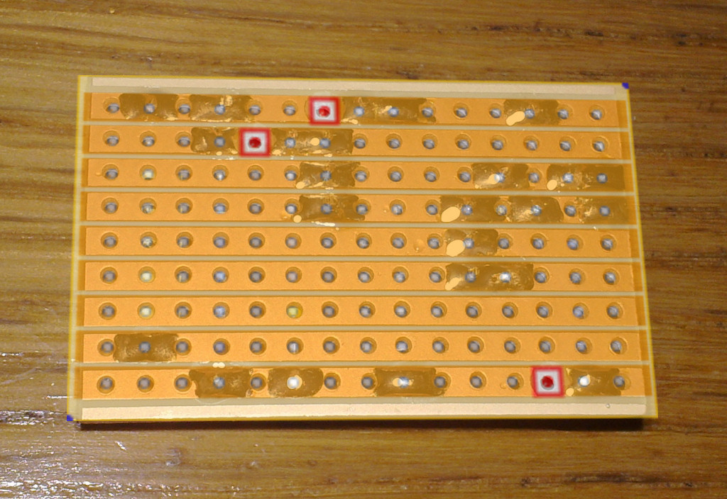
5) Checking placement and cuts

I often come across problems with builds where a part was soldered to the wrong hole, or a cut misplaced and again in most cases this would stop the effect working.  With smaller layouts it's easy enough to go over everything and double check but I use a visual method to help me check for placement errors.  Anyone who uses a graphics editing program like Photoshop or Paint Shop Pro should be able to do this easily enough, but not everyone wants to mess around with graphics programs to fault find a build, and if that is the case then just check your placements critically against the layout, counting holes to make sure everything is where it is intended to be.  You can ignore the rest of this section and skip to number 6.

I take a front and back pic of the board and then use the layout pic to create a semi transparent layer over the top.  For the top of the board just select right round the board layout and copy and paste it as a new layer over the top of the front photo. Then you can make it semi transparent by setting the layer opacity.  Then use a deformation tool to line up the layout with the photo (it's easiest to try to lineup the vero holes as points of reference).  The results make it very clear where everything should go and highlight errors


Do the same with the reverse side (don't forget to mirror the layout before pasting over the picture so it's the correct way round.


Using a filter on the track side can make it more obvious where the photo and layout cuts are.  This was using a simple "Darken" blend mode


6)  Measurements

If the above all looks good then we need something else to give us a clue to where your problem arises.  The best way to provide this is to measure the DC voltage between all transistors, ICs, regulators etc and ground.  Any voltage that isn't in the right sort of ball park will stand out like a sore thumb, so if you want help make sure you do this first to give us something to work with.

To assist you in giving us the correct information, ICs follow the following numbering convention:

1----8
2----7
3----6
4----5


and if the circuit contains transistors be sure to identify collector, base and emitter when giving voltages. 


7)  If all else fails .....

If all of the above check out ok, then the problem must be an incompetent layout designer! :o)  In this case post a message to the board including any front and back pics you've taken, along with the pin voltages mentioned in (6) and that could really help identify the problem area.

Hopefully you have more successes from this blog than failures to make the frustrations worthwhile.

Wednesday, 25 April 2012

Greeny's Vero Build Guide

A number of people have asked me to do a build guide for one of these effects, but I noticed the other day that one of the guys here (timmy) had already done a very nice one which was posted on the Ultimate Guitar forum, so I asked Tim whether we could use it here and he was happy to oblige.  So many thanks for this Tim, it's a great guide and should visually answer a lot of questions some people may have when trying build up these effects.

It may be useful to print this out for cross reference when following the guide:


Daddy, where do baby pedals come from?

Well for me, this is where. My bench. Thought i'd take some photo's of a build and show the world how i build shit.  Here we go!

Start off with this bad boy here. Vero board slab bought from Tayda Electronics.


Once you know what pedal you wanna build you find/make a layout blablahblah. I'm making a Menatone Red Snapper with IvIark's layout.

I cut it down to size and file the edges (cosmetic reasons..)


I then mark out for the trace cuts and drill a hole to start the cut.


I then grab a bigger drill bit and cut the traces by hand.


Then i add the jumpers in.


And boom, we have a board ready for components!

   
Okay so now that we have the board ready, i add components.  
I start with resistors cause they are the shortest in height. I use RN55's cause they are killer.


Then diodes. Used 1n4001's cause i love em.


I then use an IC. This is an old school JRC4558.


Then come the caps. I use Phillips ones for pedals like this for size reasons. Theres also a Silver Mica in there.


Then polarised caps. I LOVE KEMET ONES (the one that looks like a bullet) CAUSE THEY LOOK SIIIICK!


And there we have a populated board!

Now to wire it into an enclosure..
Here's one i prepared earlier!


Fill it with the required parts.


Now for wiring. I start normally with the LED and grounding.


Then input and output jacks.


Then more power/switch wiring..


Looks kinda messy at this stage. but dont panic! I then add the circuit in last!


All done!


Works a treat first time